Probing Electric Properties with Terahertz Radiation
The potential of terahertz technologies for the inspection of electronic components has long been recognized. Compared to electromagnetic radiation at other frequencies, terahertz “light” offers two distinct advantages: First, quite practically, optical inspection techniques fail when substrates or polymer-based packaging materials are opaque, yet most of these materials remain at least partly transparent in the terahertz band. Second, being able to “look” into semiconductors, terahertz measurements enable a convenient assessment of some of the essential properties of semiconductor materials, including sheet resistance, carrier density and mobility. Hence, some of the emerging applications include the contact-free characterization of coatings or even thin metal layers, quality control of solar cells, and the inspection of electronic circuits, in particular the localization of internal defects and the identification of counterfeit chips.
This application note highlights selected use cases; for a more general overview, readers are referred to ref. [1].
Sheet resistance measurements: Contact and non-contact methods
Conductive thin films have become indispensable components in electronics, being used in touch screens, displays, solar cells and transistors, to name but a few. They have to be manufactured with utmost precision in order to obtain the desired electrical properties. This requires fast, accurate and non-destructive measurements during production. One of the most relevant parameters is sheet resistance, the lateral resistance per square unit of a film, a property that denotes the ability of charge carriers to move in the plane of the film.
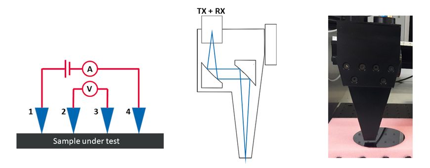
The most established technique for sheet resistance measurements uses so-called four-point probes (see Fig. 1): Four equally-spaced electrodes are brought in contact with the material to be characterized. The outer electrodes (“force leads”) apply a DC current to the sample, and the inner probes measure the corresponding voltage drop, eliminating the contribution of the force leads themselves. Common though it is, the method requires physical contact to the sample under test, and is comparatively slow.
The use of terahertz radiation offers an alternative that is not only much faster but entirely contact-free: Terahertz pulses illuminate the sample material, where they are transmitted or reflected, and finally arrive at the receiver. In today’s instruments, both the transmitter and receiver usually consist of photoconductive antennas; being fiber-coupled, they can be flexibly positioned according to the requirements of the setup. The sample properties are inferred from the terahertz reflection or transmission measurement, and comparatively simple data processing then yields the sought-after sheet resistance.
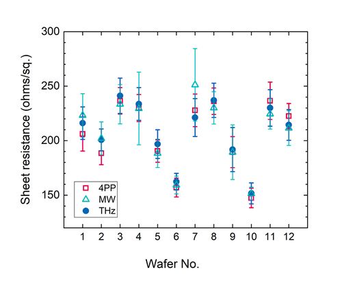
A team of researchers at National Physical Laboratory (Teddington, UK) and PragmatIC Semiconductor Limited (Cambridge, UK) recently compared various techniques for sheet resistance measurements on a set of glass wafers coated with Indium Gallium Zinc Oxide films and a thin Titanium layer. The team, led by Mira Naftaly, used four-point probes, microwave resonators and terahertz time-domain spectroscopy (THz-TDS) on the same set of samples. They proved that the different methods provided consistent values for the sheet resistance (see Fig. 2), even though the results varied significantly both between different wafers, and across the area of a single wafer [2]. For the terahertz measurements, the team employed TOPTICA’s TeraFlash pro, taking advantage of the high bandwidth and dynamic range of the THz-TDS system.
Whilst microwave resonators also enable a contact-free measurement, THz-TDS has advantages in terms of the flexibility of the mechanical arrangement, the range of conductivities that can be measured, spatial resolution, measurement speed, and a higher precision.
Flexible electronics
Non-contact measurement techniques play an equally important role in the quality control of another emerging class of electronic devices: flexible electronics. Components made of flexible circuit boards can be bent, squeezed, stretched or twisted, while retaining their electrical properties. Consequently, they are rapidly gaining attention both in high-end markets (aerospace, biomedical) as well as in consumer electronics, including even textiles and fashion.
In particular, printable electronics offer an inexpensive, yet versatile and rapidly producible alternative to conventional circuit boards. Depending on the technique chosen, the initial production step may require no more than an ink-jet printer; subsequent annealing or sintering then enhances the robustness of the print. Whilst the printing method defines the spatial resolution and determines the ultimate function of the device, the quality of the electrical properties depends critically on the post-printing annealing process.
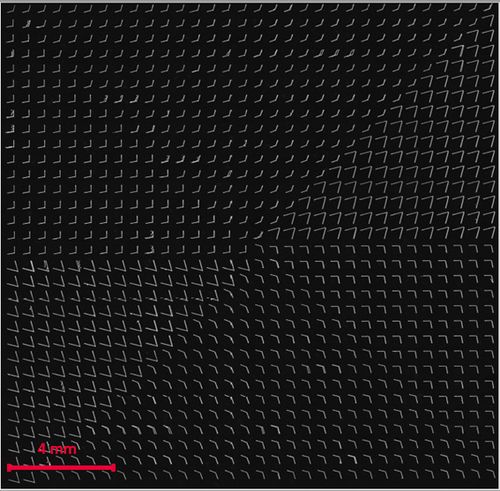
Optical inspection of printed electronics under a microscope – either an optical one, or an atomic-force microscope – works, but is time-consuming and not suitable for large-scale tests. Four-point probe methods face the same drawbacks. Again, terahertz techniques might come to the rescue. A concept published by researchers at École de Technologie Supérieure (ETS, Université du Québec, Canada) suggests the use of a terahertz “quality control bar” for the inspection of printed electronics, akin to a color control bar in graphic art printing: The control bar features a carefully designed resonant structure, so that the measurement of the terahertz transmission provides insights about the conductivity of the ink. The researchers verified that printed devices that are manufactured simultaneously with the test bar exhibited the same static conductivity [3]. Hence, the terahertz “quality control bar” eliminates the need for inspecting the entire printed structure and thus speeds up the time needed for quality screening.
Organic semiconductors
A class of materials that has attracted much interest both for the design of flexible electronics and for photovoltaics incorporates organic semiconductors. Depending on the application, it becomes crucial to understand not only the electrical, but also the thermo-mechanical properties of these materials. Much of the present research is still at a fundamental level, but the practical consequences are clear: under no circumstances should a flexible sample become rigid and brittle, just because it is winter and ambient temperatures drop.
In practice, measuring the mechanical properties of organic semiconductors has remained experimentally challenging, traditionally requiring large-scale single-crystals and intricate sample preparation.
A team of researchers led by Prof. Michael Ruggiero, University of Vermont (USA), suggested an alternative approach: they chose to investigate the underlying intermolecular forces of their samples, and used this information to obtain information on the mechanical behavior. To this end, the group combined carefully designed simulations and TD-THz spectroscopy, and investigated the thermoelastic properties of the two organic semiconductors rubrene and BTBT [4]. Probing their samples with terahertz radiation at temperatures between 100 K and 300 K, the team were able to quantify the changes in interatomic forces and, consequently, the elasticity of the materials. Both semiconductors exhibited a red-shift of their spectral signatures with increasing temperature, and the researchers were able to explain this effect with the weakening of intermolecular bonds. Put simply, the research of the Vermont team provides a better understanding of how and why the materials “soften”.
For their THz measurements, the authors used TOPTICA’s TeraFlash pro (Fig. 4), coupling the THz beam to a cryostat.
Looking into chips
Counterfeit integrated circuits (ICs) present a significant risk in security-related IT departments. In the worst case, a counterfeit IC might turn into a hardware Trojan – a maliciously modified circuit that attempts to circumvent the security features of a computer system, leaking passwords and permitting unauthorized access to the PC.
The identification of counterfeit chips proves to be costly and time-consuming. Optical inspection techniques are not applicable, as visible radiation cannot penetrate the coating or package of a chip. X-ray screening works, but makes use of ionizing radiation, with associated health and safety risks. Non-destructive testing based on terahertz radiation, whilst not facing the aforementioned challenges, has to address the question of spatial resolution: using far-field beams and conventional optics, the spot size of a terahertz beam remains limited to 0.5 .. 1 mm, not nearly sufficient to resolve the internal structures of an IC.
Researchers from Protemics GmbH (Aachen, Germany) and the Florida Institute for Cyber Security Research (Gainsville, FL, USA) recently demonstrated that terahertz near-field measurements provide a high-resolution “inside view” of ICs. They applied near-field reflection imaging to two ICs, an original and a counterfeit one, which looked identical from the outside. The terahertz image, however, revealed a significant structural difference inside the package, both of the die area around the chip and the connecting wires [5]. Earlier on, Protemics had already demonstrated that an entire graphic card with all its ICs can be inspected with the help of their near-field spectrometer (Fig. 5).
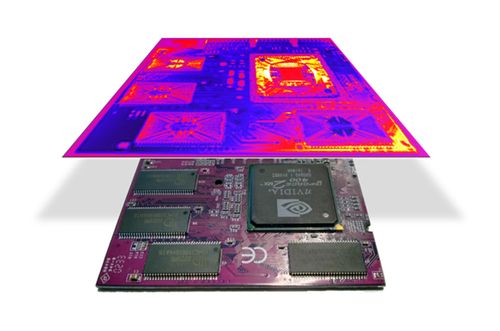
Protemics‘ near-field system combines TOPTICA’s TeraFlash pro with carefully designed microprobes, where a photoconductive switch is integrated in a cantilever design. High-resolution 3D translation stages move the sample through the terahertz beam, while keeping the microprobe at a constant vertical distance above the sample. This active control of the detector-sample distance enables measurements on arbitrary surface topographies. The spatial resolution can be as fine as 3 µm, but a lower resolution may be chosen as well (100 µm was sufficient for the inspection of counterfeit ICs, 200 µm for the graphic card in Fig. 5).
![Fig. 6: High-resolution sheet resistance map of a solar cell, obtained with a Protemics near-field terahertz system. (a) False-color representation of the sheet resistance across an area of 10 x 30 mm. (b) Close-up of the shaded area in (a). Areas with a high concentration of dopants exhibit a low sheet resistance. (c) Doping profile along the line marked in (b). From Ref. [1], figure courtesy of Protemics GmbH.](https://www.toptica.com/fileadmin/_processed_/2/8/csm_an_probing_electric_properties_thz_radiation_fig_6_c920a8391a.jpg)
Conductivity mapping of solar cells
One of the striking features of Protemics’ near-field system is that the complete pulse trace and hence, time-domain and frequency-domain information is preserved for each image pixel. Therefore, the insights that can be gained from a near-field image go far beyond mere amplitude or phase representations: Users may choose to retrieve depth information and compute layer profiles, or process the data to obtain maps of sheet resistance, conductivity or carrier mobility. In short, all of the sample properties mentioned at the beginning can be measured quantitatively and with sub-wavelength resolution.
Figure 6 depicts a high-resolution map of the sheet resistance of a section of a solar cell, computed from a terahertz near-field image. Blue and red sections correspond to regions with low and high resistance, respectively. Whilst the sheet resistance is “mostly” low, some regions in the top-left corner of Fig. 6(a) exhibit an unusually high sheet resistance, with values close to 600 W/sq. Vice versa, the close-up in Fig. 6(b) shows that the sheet resistance is particularly low in regions that are heavily doped (n++ and p++), in accordance with the doping profile sketched in Fig. 6(c).
The example illustrates how parameter maps obtained with terahertz near-field measurements may prove beneficial in the quality control of semiconductors, and help in identifying faults in individual devices.
Conclusion
Quality control of displays and touch screens, protection against product piracy in chip manufacturing, efficiency improvements in flexible electronics, identification of defects in solar cells, fundamental research on novel semiconductors and their properties: there is an ever-increasing need for fast, reliable and non-destructive methods for quality assurance in the production of electric and electronic components. An ideal system should be affordable, long-lived, precise, able to operate in a non-contact way and “autonomous” in the sense that it does not require the presence of a technical expert. Modern time-domain terahertz systems have risen to the challenge and have shown their potential to provide a wealth of information on central properties of both raw semiconductor materials and packaged electronic components. First industrial installations already make use of terahertz-based techniques, and many more are expected to follow.
Acknowledgement
TOPTICA Photonics would like to thank Dr. Mira Naftaly (NPL), Prof. François Blanchard (ETS Québec) and Dr. Michael Nagel (Protemics) for their contributions and valuable discussions.
[1] M. Naftaly, N. Vieweg, A. Deninger: Industrial applications of terahertz sensing: State of play; MDPI Sensors 19 (2019) 4203; doi:10.3390/s19194203.
[2] M. Naftaly, S. Das, J. Gallop, K. Pan, F. Alkhalil, D. Kariyapperuma, S. Constant, C. Ramsdale. L. Hao: Sheet resistance measurements of conductive thin films: a comparison of techniques; Electronics 10 (2021) 960; doi.org/10.3390/electronics10080960.
[3] M. Zhuldybina, X. Ropagnol, C. Trudeau, M. Bolduc, R.J. Zednik, F. Blanchard: Contactless in situ electrical characterization method of printed electronic devices with terahertz spectroscopy; MDPI Sensors 19 (2019) 444; doi:10.3390/s19030444.
[4] P.A. Banks, J. Maul, M.T. Mancini, A.C. Whalley, A. Erba, M.T. Ruggiero: Thermoelasticity in organic semiconductors determined with terahertz spectroscopy and quantum quasi-harmonic simulations; J. Materials Chemistry C (2020). DOI: 10.1039/d0tc01676d
[5] A. Michalski, S. Sawallich, J. True, N. Asadizanjani, M. Nagel: High-resolution terahertz near-field reflection measurements for complementary non-destructive inspection of integrated circuits; Proc. IRMMW-THz 2021.

